ATtiny10 PeripherieATtiny10 Peripherie
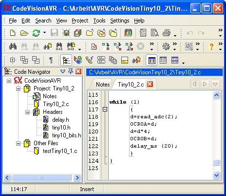
Eine Besonderheit des Tiny10 ist sein AD-Wandler
mit einer Auflösung von nur 8 Bit. Dafür ist aber der Timer 0
mit 16 Bit besser ausgestattet als beim Tiny13. Das folgende Programm
testet AD und 10-Bit-PWM. An B2 wird eine Spannung gemessen und einmal
als 8-Bit-Wert (bis 25%) am ersten PWM-Ausgang ausgegeben, und dann
noch einmal mit 10 Bit (100%) am zweiten. Das Projekt zeigt auch die
Delay-Funktion in CodeVision. Ich warte 20 ms, damit der Messtakt nahe
bei 50 Hz liegt. Am Ausgang sieht man dann auch 50-Hz-Anteile der
Messspannung als langsame Schwankungen.
/*****************************************************Download: CodeVisionTiny10_2.zip
This program was produced by the
CodeWizardAVR V2.04.9a Evaluation
Automatic Program Generator
© Copyright 1998-2010 Pavel Haiduc, HP InfoTech s.r.l.
http://www.hpinfotech.com
Project :
Version :
Date : 05.11.2010
Author : Freeware, for evaluation and non-commercial use only
Company :
Comments:
Chip type : ATtiny10
AVR Core Clock frequency: 1,000000 MHz
Memory model : Tiny
External RAM size : 0
Data Stack size : 8
*****************************************************/
#include <tiny10.h>
#include <delay.h>
// Read the AD conversion result
unsigned char read_adc(unsigned char adc_input)
{
ADMUX=adc_input & 0x03;
// Delay needed for the stabilization of the ADC input voltage
delay_us(10);
// Start the AD conversion
ADCSRA|=0x40;
// Wait for the AD conversion to complete
while ((ADCSRA & 0x10)==0);
ADCSRA|=0x10;
return ADCL;
}
// Declare your global variables here
int d;
void main(void)
{
// Declare your local variables here
// Main Clock source: Calibrated Internal 8 MHz Osc.
#pragma optsize-
CCP=0xD8;
CLKMSR=0x00;
// Clock Prescaler division factor: 8
CCP=0xD8;
CLKPSR=0x03;
#ifdef _OPTIMIZE_SIZE_
#pragma optsize+
#endif
// Voltage Level Monitor
// Trigger Level: Voltage Level Monitor Disabled
// Interrupt: Off
VLMCSR=0x00;
// Input/Output Ports initialization
// Port B initialization
// Pull-up initialization
PUEB=0x00;
// Func3=In Func2=In Func1=Out Func0=Out
// State3=T State2=T State1=0 State0=0
PORTB=0x00;
DDRB=0x03;
// Break Before Make Mode PORTB: Off
PORTCR=0x00;
// Timer/Counter 0 initialization
// Clock source: System Clock
// Clock value: 1000,000 kHz
// Mode: Ph. correct PWM top=0x03FF
// Input Capture on Falling Edge
// Input Capture Noise Canceler: Off
// OC0A output: Non-Inverted
// OC0B output: Non-Inverted
TCCR0A=0xA3;
TCCR0B=0x01;
TCNT0=0x0000;
ICR0=0x0000;
OCR0A=0x0000;
OCR0B=0x0000;
// External Interrupt(s) initialization
// INT0: Off
// Interrupt on any change on pins PCINT0-3: Off
EICRA=0x00;
EIMSK=0x00;
PCICR=0x00;
// Timer/Counter 0 Interrupt(s) initialization
TIMSK0=0x00;
// Analog Comparator initialization
// Analog Comparator: Off
// Analog Comparator Input Capture by Timer/Counter 0: Off
ACSR=0x80;
// ADC initialization
// ADC Clock frequency: 500,000 kHz
// ADC Auto Trigger Source: ADC Stopped
// Digital input buffers on ADC0: On, ADC1: On, ADC2: On, ADC3: On
DIDR0=0x00;
ADCSRA=0x81;
ADCSRB=0x00;
while (1)
{
d=read_adc(2);
OCR0A=d;
d=d*4;
OCR0B=d;
delay_ms (20);
}
}
// Input/Output Ports initializationNoch etwas ist neu: Man kann auf das PINB-Register Einsen schreiben und bewirkt damit, dass die entsprechenden Ausgangszustände toggeln! Das ist zwar auf den ersten Blick unlogisch, kann aber sehr praktisch sein. Weil das in der Form nur mit den kleinen Tinys geht, musste ich es gleich mal ausprobieren. Das Ergebnis ist ein symmetrisches Rechecksignal an allen Pins.
// Port B initialization
// Pull-up initialization
PUEB=0x00;
// Func3=In Func2=Out Func1=Out Func0=Out
// State3=T State2=0 State1=0 State0=0
PORTB=0x00;
DDRB=0x07;
while (1)
      {
      PINB=0x07;
      delay_us (10);
      }